Table Of Content

Basic tasks are easy to perform, but advanced features are only a few clicks away, ensuring you can get designing quickly but won’t be limited down the line as you develop your design skills. It was developed by Jean-Pierre Charras from the Grenoble IUT in France in 1992. This design software includes diagram management, PCB routing and 3D modelling possibilities for electronics engineers. With this PCB board design software, you can quickly test ideas and check circuit performance using SPICE simulation methods. All changes are automatically synchronized between your layout and models, so you can fully focus on the creative process. KiCAD EDA is an open-source and cross-platform electronics design automation platform.
The Community for Creative Electronics
These downloads include everything from diagramming and drawing tools to PCB design applications that can help you develop a streamlined design process. Moreover, use constraint management to ensure your design meets certain requirements based on region, pair, length rules, etc. You can also make a bridge between MCAD and ECAD flows to get a perfect design environment according to your needs with the support for STEP, IDX, and IPC-2581.
Altium Designer 24: From Requested to Required
These design rules collectively cover every aspect of a design, and they form a set of instructions for the PCB editor to follow. Your printed circuit routing widths, clearances, plane connection styles, routing via styles, and other design rules can be monitored in real-time by the online design rule checker (DRC). Altium Designer rules are not attributes of the objects, they are defined independently of objects in a circuit board.
Uploading your EAGLE Files for Manufacture
TinyCAD supports PCB layout programs with multiple connection list formats. It can also create SPICE simulation lists and comes with character libraries. Are you looking for free PCB design software to implement your new electronic project? Check out this list of 12 free PCB software using which you will be able to design your printed circuit board quicker and without many hours of learning. Get a comprehensive PCB design solution with OrCAD PCB Designer that provides route technology and an advanced platform. It contains technologies like librarian tools, signal integrity, auto-routing, constraint manager, schematic capture, PCB editing, routing, and mixed-signal circuit simulation.
To start designing your custom printed circuit boards, download the appropriate software version below and follow our step-by-step tutorial that walks you through the entire design process. Printed circuit boards (PCBs) are ubiquitous in electronics and make up a substantial fraction of environmentally hazardous electronic waste when devices reach end-of-life. Their recycling is challenging due to their use of irreversibly cured thermoset epoxies in manufacturing. Here, to tackle this challenge, we present a PCB formulation using transesterification vitrimers (vPCBs) and an end-to-end fabrication process compatible with standard manufacturing ecosystems.
Just like KiCAD, Fritzing is an open-source platform for learning electronics. Fritzing became popular with its examples of Arduino and its an easy to use platform. Fritzing includes a breadboard layout, schematic, and PCB view for designing a PCB layout for your board. With a rich interface and growing community, fritzing is a good choice among hobbyists.
Establish a digital thread that seamlessly connects the entire system, including subsystems and functional partitions across multiple engineering domains, on a unified platform. Furthermore, KiCad EDA has a built-in raytracer along with customizable lighting options so that you can create true images and share them with your colleagues or teams to show your work. This software also supports various OS, such as Ubuntu, macOS, Windows, Debian, Arch Linux, FreeBSD, Fedora, etc. Start with a full-featured 30-days free trial, which is now available in Windows 32, Windows 64, and macOS.
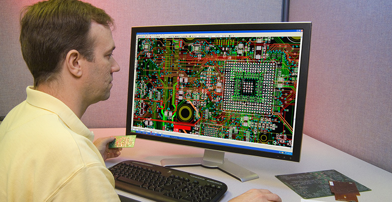
For over 25 years, we’ve provided one of the easiest to learn, design, and direct order ecosystems for professionals and students alike. When routing any noisy ground traces, be sure to keep them as far away as possible from signals that need some peace and quiet. You can also place a ground plane directly under noisy signal traces to lower the impedance for high-speed designs. The schematic editor and printed circuit layout features in Altium Designer. Try any of the above PCB design software downloads and start your free trial of Altium Designer. For PCB design, users need a specialized CAD application that includes circuit creation tools and is tailored for PCB layout.
Step 6: Place Components
Net names can be assigned in the schematics to help you stay organized. Take advantage of the view configuration features to quickly find what you need. Our dedicated PCB software allows you to design PCBS in hours without extensive and expensive training. I’m trying PCB Artist from Advance circuits now,Schematic capture seems to work well.
Our cradle-to-cradle life-cycle assessment shows substantial environmental impact reduction of the vPCBs over conventional PCBs in 11 categories. We successfully manufactured functional prototypes of Internet of Things devices transmitting 2.4 GHz radio signals on vPCBs with electrical and mechanical properties meeting industry standards. Fractures and holes in vPCBs are repairable while retaining comparable performance over multiple repair cycles. We further demonstrate a non-destructive recycling process based on polymer swelling with small-molecule solvents.
PCB Stator Technology at Automate 2023 - Machine Design
PCB Stator Technology at Automate 2023.
Posted: Tue, 23 May 2023 07:00:00 GMT [source]
These capabilities help you improve your PCB design’s quality and result in high-quality printed circuit board (PCB) manufacturing. KiCad features a schematic editor, suitable for everything from simple designs all the way to complex multi-sheet projects. The editor also has an integrated SPICE simulator for testing the viability of circuits before porting them to the real world.
Before laying down any of your traces, be sure to use a trace width calculator (thanks, Advanced Circuits). Using this calculator will help you to easily determine how thick and wide all of your traces will need to be based on your specific design requirements. And if you end up having extra space on your board, go ahead and use traces with wider widths, as this won’t cost extra from your manufacturer. When placing your components always be mindful of how long your traces are going to need to be to connect your pins together.
PCBs—which house and interconnect chips, transistors, and other components—typically consist of layers of thin glass fiber sheets coated in hard plastic and laminated together with copper. That plastic can't easily be separated from the glass, so PCBs often pile up in landfills, where their chemicals can seep into the environment. By requesting ExpressPCB Plus you are agreeing to receive email regarding software and product updates, industry news and discount codes from ExpressPCB.
The PCB layout design features make component placement and routing easy. Altium Designer’s rules-driven design engine is a huge advance over free PCB design and layout software. Advanced circuit boards require more powerful PCB design tools than what you’ll find in free circuit layout software. When you’re dealing with multi-board assemblies and high-density routing, your PCB layout design software should help you expedite your designs and quickly create new circuit boards without using multiple programs. With Altium Designer, you can define multiple boards in the schematic editor, and you can quickly route high-speed designs with advanced PCB design tools. No other circuit board drawing software provides this level of functionality.


No comments:
Post a Comment